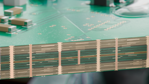
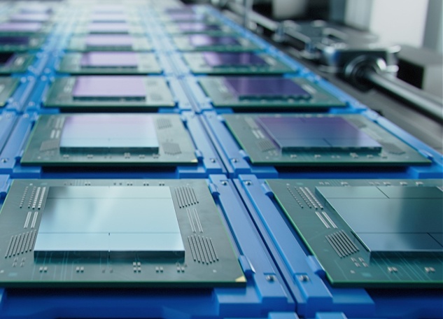
互连 我们的先进互连解决方案可确保强大可靠的连接。 提供无缝电导性能 我们的金属化和晶圆级封装技术可实现复杂的高密度互连设计。我们为印刷电路板的直接金属化、IC载板上的半加成铜金属化以及 TSV 互连的镀铜提供先进的解决方案。我们的集成金属化技术包括高精度 RDL 电镀和过孔填充、无空洞精细大马士革工艺、键合、铜柱电镀和背面金属化。当应用于晶圆级封装、印刷电路板制造和半导体组装时,我们的解决方案可提供无缝电导性能和长期可靠性,体现我们在互连领域的创新能力和卓越的互连性能。 面向电子供应链各阶段的解决方案 精密互连:利用金属化解决方案推进晶圆级封装 互连 Interconnect Interconnecting with Precision: Advancing Wafer-Level Packaging with Metallization Solutions Hybrid BondingHybrid bonding technology such as NOVAFAB® and MICROFAB® enables scalability, pitch reduction, and increased interconnect density, while enhancing performance, reliability, and thermal dissipation. Backside MetallizationBackside metallization like NOVAFAB® enables heat removal from SiC, GaN, or GaAs dies used in power and RF components and provides an active surface for sintered die attach materials. Through Silicon Via (TSV)Through silicon via (TSV) interconnects enable high-performance 2.5D and 3D packaging, improving integration, electrical performance, and die-to-die communication with technology like MICROFAB®. Direct MetallizationDirect metallization technology like Shadow® selectively applies carbon to substrates and vias, enhancing efficiency and reliability, replacing electroless copper, and eliminating formaldehyde. IC SubstrateSemi-additive copper metallization processes like Systek® yield 100% throwing power without formaldehyde, enabling high-density circuitry and simultaneous micro via filling and trace plating. DamasceneViaForm® damascene facilitates void-free fine-feature copper interconnects deposited into etched patterns and vias within dielectric layers, enabling high-density interconnects for circuits. Redistribution Layer (RDL)Metallization technology like Systek® for redistribution layers (RDL) is vital to reroute connections and enable high-density heterogeneous integration via wafer-level fan out, 3D, and 2.5D packaging. Copper PillarMacDermid Enthone® copper pillar plating technology is used for flip chip interconnects, reducing pitch down to 20µm, boosting electromigration performance, and meeting RoHS/Green initiatives. 推动性能、效率和可持续发展 提升性能 我们的集成解决方案通过减少间距、支持 2.5D 和 3D 封装、提高密度、实现 100% 均掷力以及促进异构集成而提升性能。 优化热管理 为了有效散热,重要的是要解决组件多个方面的热挑战。在上图中,我们重点介绍了背面金属化和键合技术如何实现优异的热管理。 推动可持续发展 我们通过不含贵金属的初级金属化技术满足 RoHS 标准、剔除受限材料并减少资源使用,以此实现可持续的印刷电路板制造。 相关解决方案 半导体组装 为电子产品、光掩膜、贴片、封装和摄像头模组提供可靠的粘结材料,推动创新型电子产品发展。 了解更多 晶圆级封装 通过先进的晶圆级封装技术,支持创新半导体设计,提升计算机芯片的性能和可靠性。 了解更多 电子线路解决方案 利用创新型特种化学品和材料,为复杂的印刷电路板和集成电路基板设计提供新一代技术。 了解更多 常见问题 “如何在复杂的多层电子设计中确保高可靠性互连?” 现代互连技术需求对传统材料提出更高要求 - 如缺乏更先进的解决方案,可能会在关键应用中引发信号完整性问题、分层或性能失效等情况。 还在寻找解决方案?我们可以提供帮助。 联系我们 了解更多 查看我们的产品 了解更多 查看资源中心 了解更多